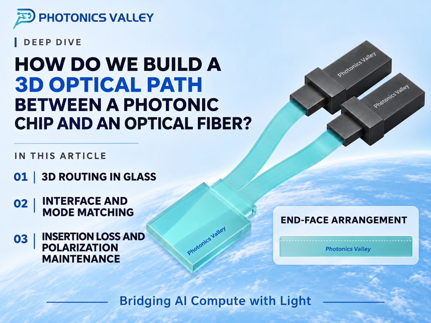
Glass can do more than transmit light. It can also contain three-dimensional pathways that guide light through its interior.
Using femtosecond laser direct writing, PHOTONICS VALLEY creates optical waveguides inside glass, allowing multiple optical signals to travel along designed paths. These paths can bend, run at different depths, and rearrange channels in three-dimensional space, offering greater design flexibility for high-density connections between photonic integrated circuits (PICs) and optical fiber interfaces.
How are these optical paths “written” inside glass? And what connection challenges can this technology address?
What Are Femtosecond Laser Direct-Written 3D Optical Waveguides?
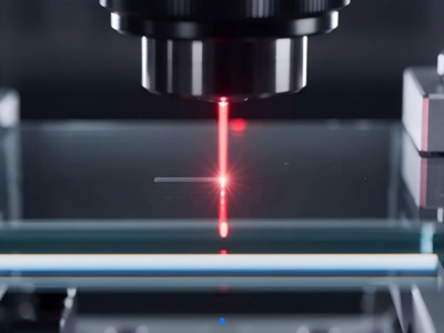
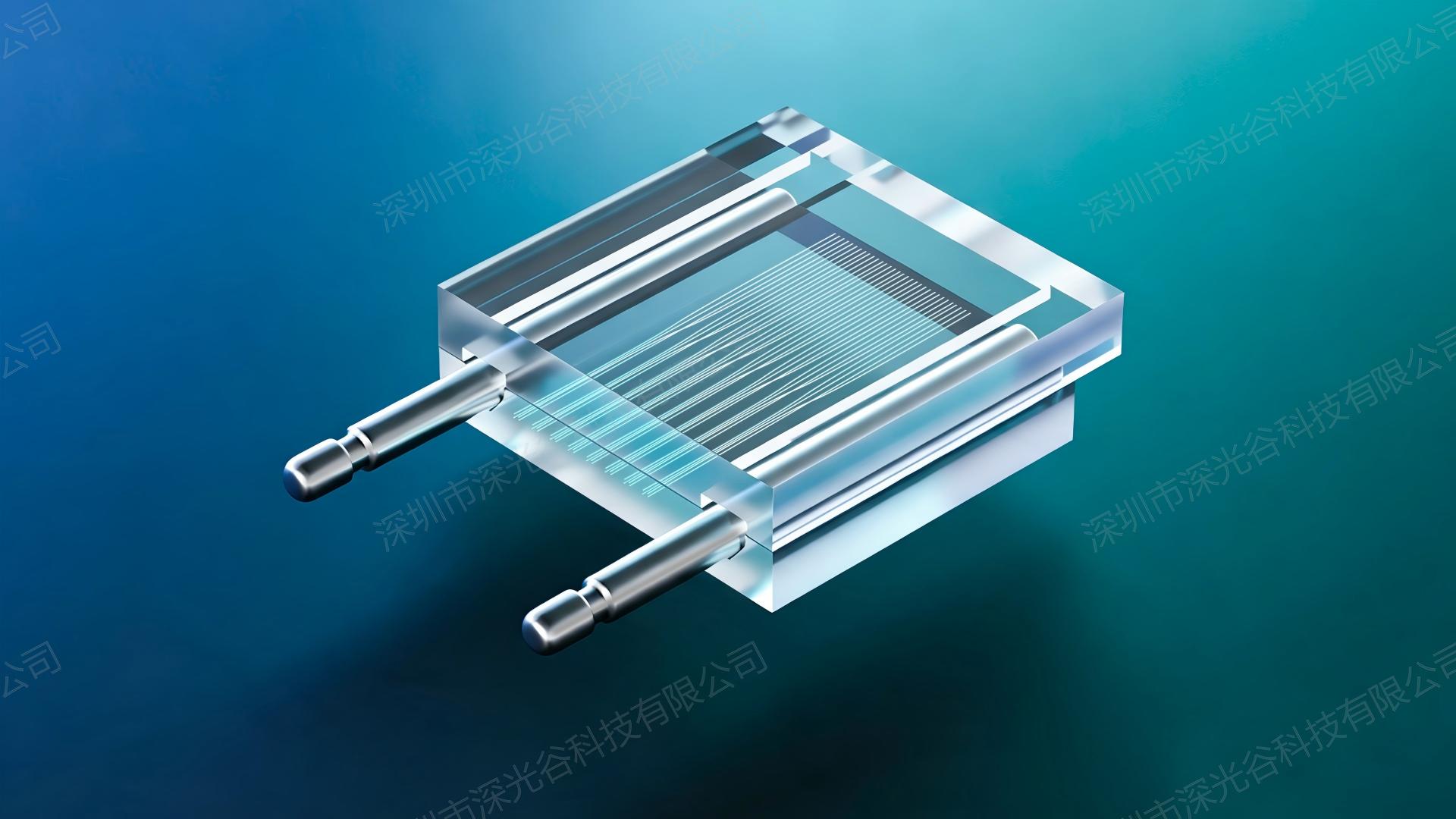
Femtosecond laser direct writing uses a focused femtosecond laser to create structures that guide light along predefined paths inside glass.
Think of the laser focus as a “pen” moving through the glass: the designed trajectory determines the route of the optical waveguide. Once fabrication is complete, optical signals travel through the resulting waveguide.
Here, “writing” means creating a light-guiding structure within the glass. It does not mean engraving grooves on the surface or embedding optical fibers in the material.
“3D” means that optical paths can be designed throughout the glass volume. Multiple channels do not have to remain in a single plane. Instead, paths at different depths and with different trajectories can connect the input and output interfaces.
From a Laser Focus to Three-Dimensional Optical Paths
The fabrication of femtosecond laser direct-written 3D optical waveguides can be divided into three stages.
First, define the connection requirements at both ends. How many input and output channels are needed? How are the channels arranged? Do the interfaces have the same channel spacing? Together, these requirements determine the optical path design.
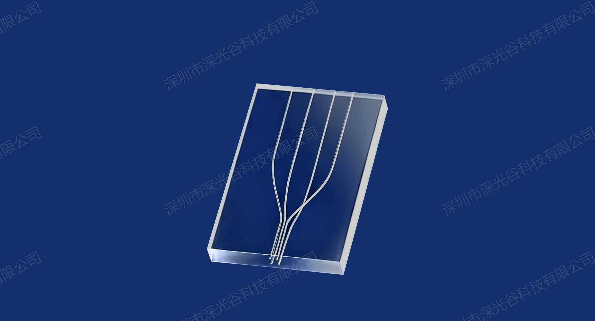
Next, focus the laser inside the glass. As the focal point moves along the designed trajectory, it progressively forms an optical waveguide. Writing multiple paths creates a multichannel interconnect structure within a single piece of glass.
Finally, route the optical channels to the required output arrangement. Optical signals enter at the input, travel along their respective three-dimensional paths, and exit at the corresponding positions to connect to the next chip or fiber interface.
The value of this technology therefore extends beyond allowing light to pass through glass. It enables the path from one position to another to be designed around the requirements of the two interfaces.
Why Do Optical Interconnects Need Three-Dimensional Routing?
The interfaces at either end of an optical interconnect do not always share the same layout.
For example, one end may consist of closely spaced PIC optical channels, while the other is a fiber array with a different pitch. Another application may require a linear row of channels to be rearranged to match the core positions of a multicore fiber.
In these cases, the connection requires more than alignment at both ends. It also requires a transition between different spatial layouts. Glass-based 3D optical waveguides can use three-dimensional routing to perform the following functions:
Channel rearrangement: Transform the input channel arrangement into the layout required at the output.
Pitch conversion: Connect interfaces with different channel spacings.
Fan-in and fan-out: Bring channels from a more widely spaced arrangement into a compact layout, or spread closely spaced channels into a wider arrangement.
The ability to bend paths, route them at different depths, and cross them in three-dimensional space provides design flexibility for these transitions. Each path must still be designed according to device dimensions, optical performance requirements, and interface specifications.
Application 1: Connecting PICs to Multicore Fibers
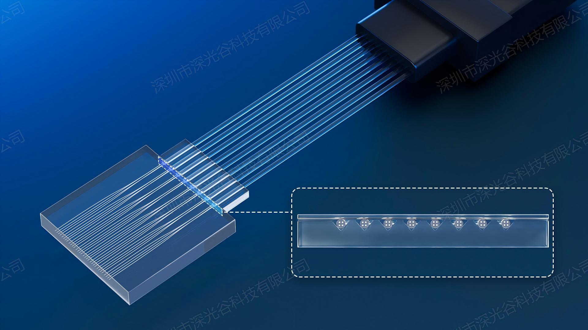
A multicore fiber contains multiple individual cores within a single optical fiber. Taking a four-core fiber as an example, the same number of channels could theoretically be carried using approximately 75% fewer fibers than a configuration in which each single-core fiber carries one channel.
To use these cores, however, each optical signal must be connected to its corresponding core position.
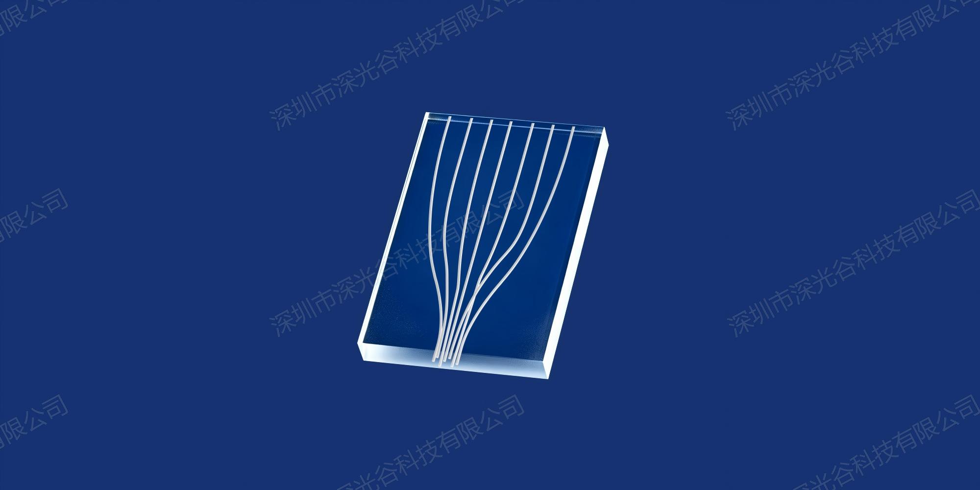
Between a PIC and a multicore fiber, 3D optical waveguides can rearrange the channels. They receive multiple optical signals from the PIC, route them through the glass, and couple each channel into a different core of the multicore fiber.
The connection can be summarized as:
PIC → Glass-Based 3D Optical Waveguides → Multicore Fiber (MCF)
In this structure, the 3D optical waveguides bridge the different channel layouts at the two interfaces.
Application 2: High-Density Optical Connections for NPO and CPO
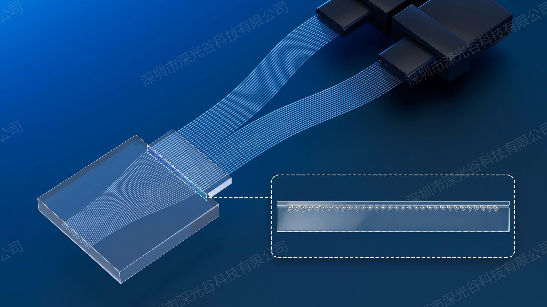
In near-packaged optics (NPO) and co-packaged optics (CPO) architectures, increasing channel counts and tighter interface spacing place greater demands on the spatial layout of optical connections.
Between a PIC and a fiber interface, glass-based 3D optical waveguides can provide fan-in, fan-out, and pitch conversion to connect optical channels with different densities and arrangements.
Their role in a system can be understood through a practical question: when the channel arrangement on the chip differs from that at the fiber interface, how can the connection be made within a limited space? Three-dimensional optical routing offers one technical approach to this challenge.
Glass-Based 3D Optical Waveguide Technology at PHOTONICS VALLEY
PHOTONICS VALLEY uses femtosecond laser direct writing to create three-dimensional optical waveguides inside glass, designing optical interconnects for requirements such as high-density optical coupling, channel rearrangement, and interface pitch conversion.
From a single optical path inside glass to multichannel connections between PICs and multicore fibers, femtosecond laser direct writing makes the spatial arrangement of optical paths a configurable device function.
If your project involves PIC-to-fiber connections, multicore fiber coupling, or high-density optical routing for NPO/CPO, contact PHOTONICS VALLEY to discuss your channel count, interface layout, and target pitch, and explore suitable glass-based 3D optical waveguide solutions.
Contact Us
Address: Room 825, Tower B, Building 12, Shenzhen Bay Science and Technology Eco-Park, No. 18 Keji South Road, High-Tech Zone Community, Yuehai Subdistrict, Nanshan District, Shenzhen, Guangdong, China
Tel: +86-755-84652252
Mobile: +86-189 4877 6698
Email: info@photonicsv.com
Website: www.photonicsv.com