Connecting a photonic chip to an optical fiber raises several design questions. How do the channels at each end map to one another? Do their pitches match? Can the optical fields couple efficiently? How much light is lost along the path and at the interfaces?
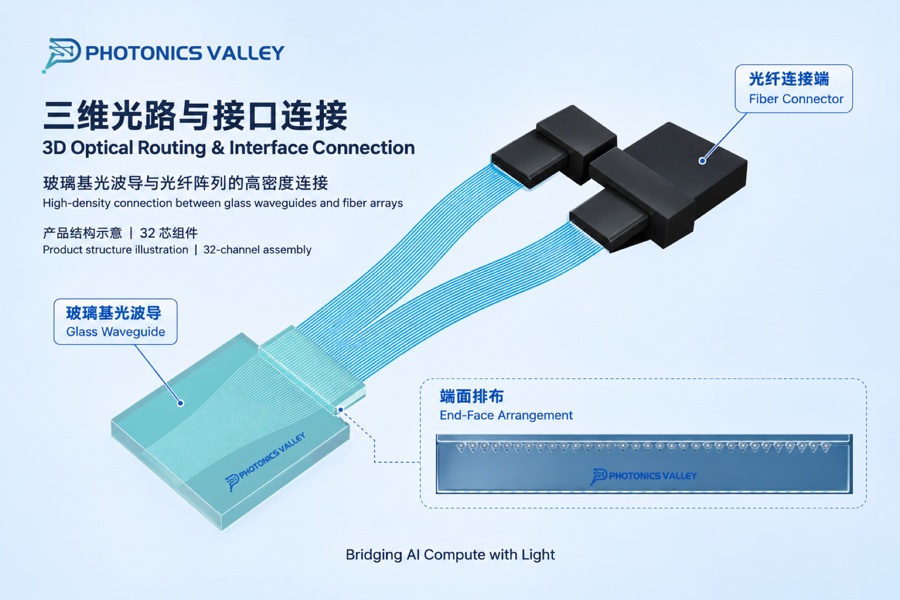
As interfaces move from single-row to multi-row arrays and channel counts rise, optical routing becomes more complex. Glass-based 3D optical waveguides provide a way to route light through the volume of the glass, where individual paths can be arranged to match the channel layouts at both ends.
PHOTONICS VALLEY combines femtosecond laser direct writing with waveguide cross-section and mode-field design, end-face preparation, and optical coupling to support applications in optical modules, co-packaged optics (CPO), near-packaged optics (NPO), and optical interconnects.
Figure 1 | 3D Optical Routing and Interface Connection
01 | Writing Optical Paths Inside Glass with a Femtosecond Laser
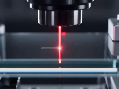
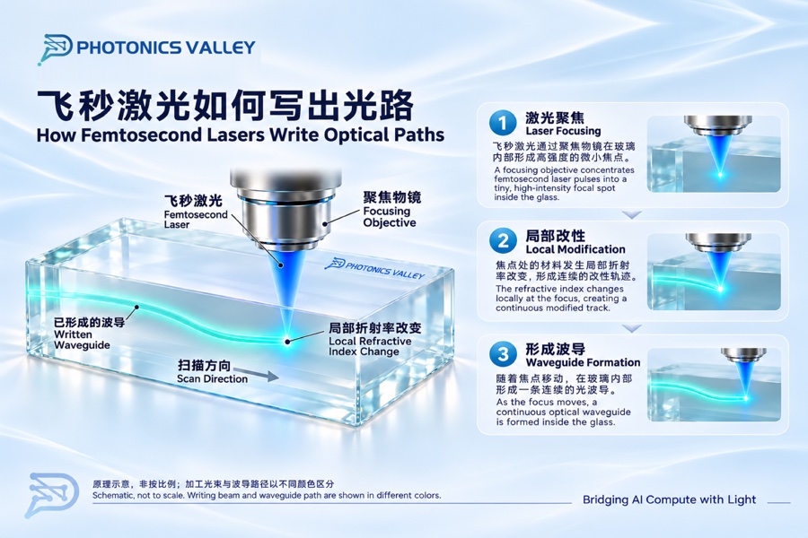
Femtosecond laser direct writing uses a focused laser to induce a localized change in the refractive index of glass. Moving the focal point along a designed trajectory creates a waveguide that confines and guides light.
Because the focal point can move in three dimensions, individual channels can be routed at different depths. This gives designers room to turn optical paths and map channels between different array layouts while meeting the optical constraints of each path.
PHOTONICS VALLEY uses a proprietary single-pass writing process to form the designed waveguide paths inside glass. The process controls the trajectory and cross-section together with the optical properties needed for transmission and interface coupling. Measurements of loss, mode-field characteristics, and polarization behavior help determine whether the fabricated waveguide meets the application requirements.
Figure 2 | How Femtosecond Laser Direct Writing Forms a Waveguide
02 | Designing the Route and Matching the Optical Fields
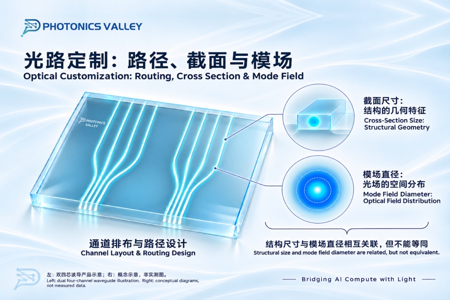
The geometry of the two interfaces determines where each waveguide path starts and ends. Devices can differ in channel pitch, channel density, array layout, and interface height. The route must account for all four.
Once the channels are aligned, coupling efficiency also depends on how well the optical fields overlap. The waveguide cross-section, refractive-index profile, and mode-field characteristics all affect that overlap.
PHOTONICS VALLEY’s direct-writing process supports circular waveguide cross-sections with controlled dimensions and customizable mode-field diameters. Cross-sectional dimensions describe the geometry of the waveguide structure. Mode-field diameter describes the spatial extent of the guided optical field. Both are useful when designing an interface.
Waveguides can also be designed for applications that require higher-order modes. The cross-section, mode field, and supported modes are selected together based on the operating wavelength and the target interfaces.
Figure 3 | Optical Routing, Waveguide Cross-Section, and Mode Field
03 | Understanding Propagation Loss, Coupling Loss, and Return Loss
Light couples into the waveguide, travels along it, and couples out into the next device. Each step affects how much optical power reaches the output. The interfaces can also reflect some light back toward the input.
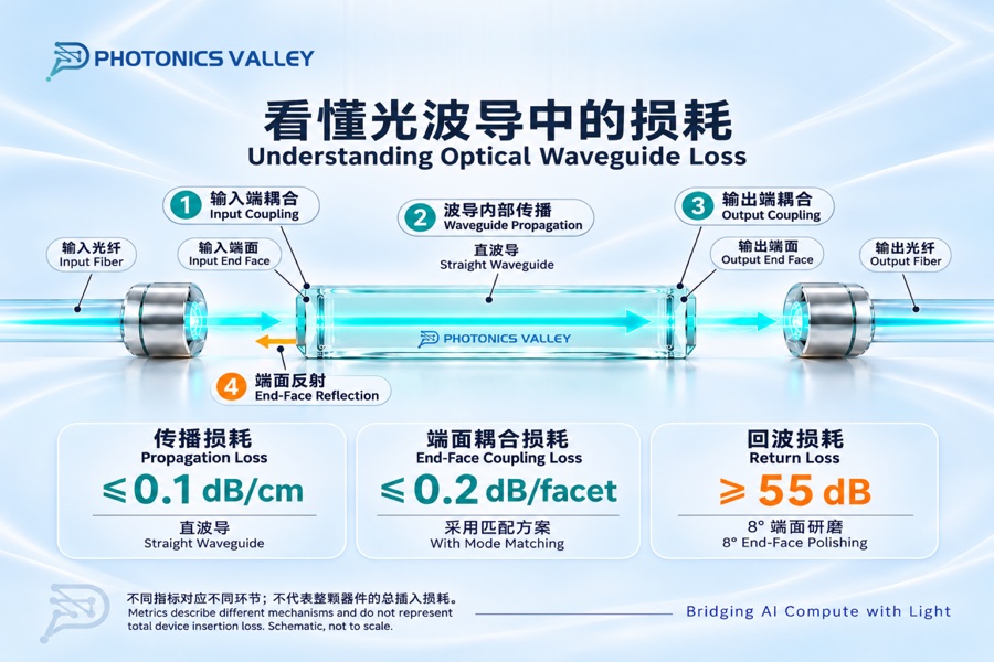
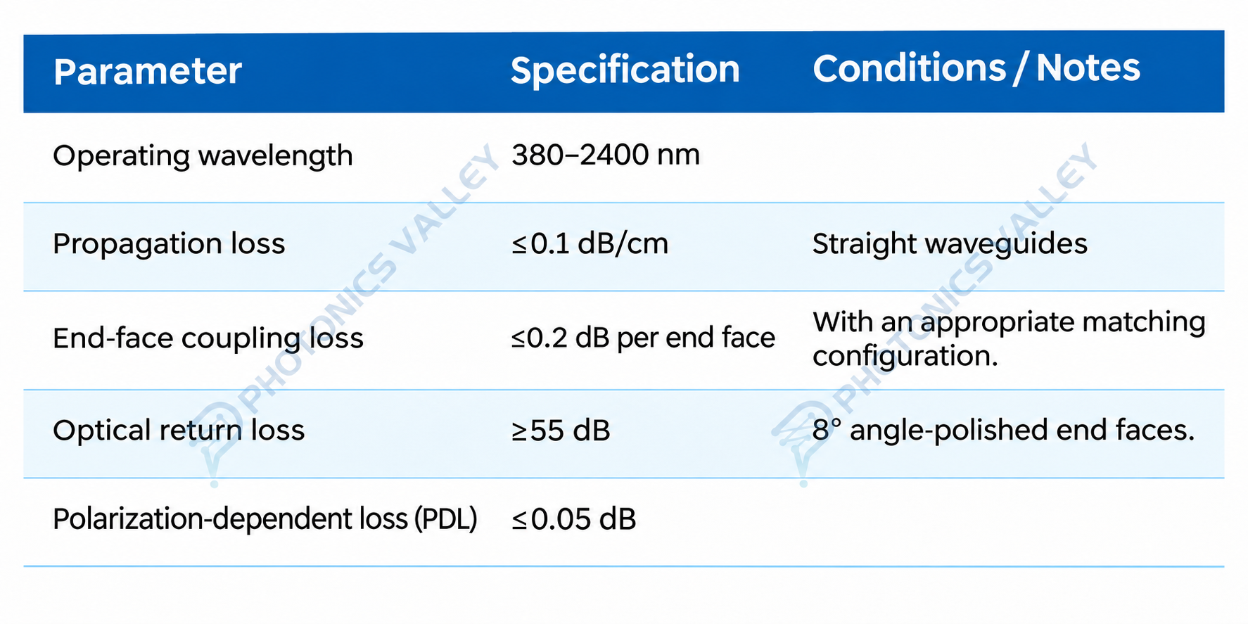
Propagation loss measures attenuation along the waveguide and is typically expressed in dB/cm. PHOTONICS VALLEY’s product literature lists a propagation loss of ≤0.1 dB/cm for straight waveguides. A 3D route must be evaluated based on its length, bends, and geometry.
End-face coupling loss measures how much optical power is lost when light enters or leaves the waveguide at an interface. It depends on mode-field matching, alignment, and end-face preparation. With an appropriate matching configuration, the specified coupling loss is ≤0.2 dB per end face.
Optical return loss measures how much light is reflected back toward the input relative to the incident light. The specified return loss is ≥55 dB with 8° angle-polished end faces. A higher return loss means less light is reflected back.
To determine the overall insertion loss of a device, measure the complete optical path, including both interfaces.
Figure 4 | Propagation Loss, End-Face Coupling Loss, and Optical Return Loss
04 | Operating Wavelength, Polarization, and Stability
The operating wavelength range listed in PHOTONICS VALLEY’s product literature is 380–2400 nm, spanning multiple bands from the visible to the near-infrared. Glass transmission in these bands makes it possible to design waveguides for different wavelengths. Each device is designed and validated at its target wavelength and under the relevant operating conditions.
Polarization-sensitive applications require separate assessments of polarization-dependent loss (PDL) and polarization maintenance. PDL measures how much loss varies with the input polarization state. The specified PDL is ≤0.05 dB. Polarization maintenance describes how well the waveguide preserves the required polarization state during transmission and is evaluated under the conditions of the intended application.
PHOTONICS VALLEY’s glass-based 3D optical waveguides offer polarization-maintaining characteristics. If a waveguide section meets the system’s polarization requirements at the target wavelength and under the actual coupling conditions, it can handle part of the transmission that would otherwise require polarization-maintaining fiber. This can reduce the use of polarization-maintaining fiber inside the package.
Dimensional, thermal, and chemical stability support the waveguide structure and its integration into a package. The environmental limits and reliability requirements for each device should be reflected in its validation conditions.
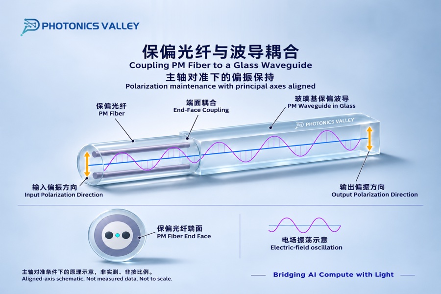
Table | Key Specifications and Applicable Conditions
The specifications are drawn from PHOTONICS VALLEY’s product literature. Whether a particular model meets them simultaneously depends on the operating wavelength and test conditions.
05 | Integration with TGV Technology and Silicon Photonics
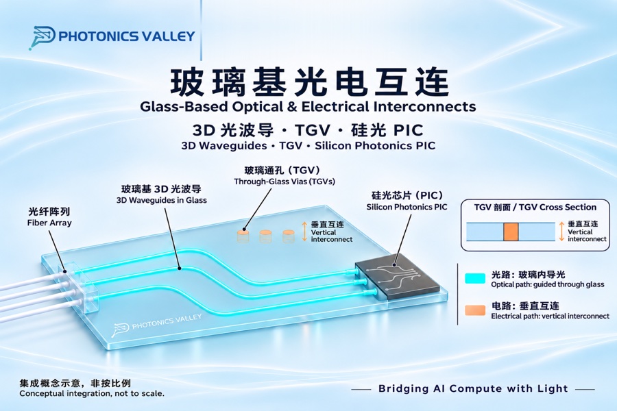
At the system level, waveguides work alongside chips, substrates, and connector assemblies. PHOTONICS VALLEY’s glass-based 3D waveguide solution is compatible with through-glass via (TGV) technology and silicon photonics process platforms.
The waveguides route light through the glass, while TGVs provide electrical connections through the glass substrate. Integrating both into one package requires coordination of the optical interfaces, electrical connections, and physical layout.
For silicon photonics applications, the waveguide route and coupling interfaces must also account for the layout and requirements of the photonic integrated circuit (PIC). The final connection design depends on the chip and the packaging approach.
06 | From Waveguide Chips to Optical Interconnects
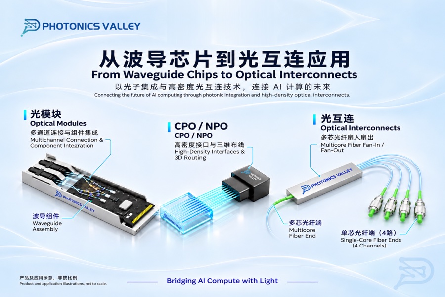
In optical modules, waveguide chips and connector assemblies can route multiple channels and convert between interface layouts. PHOTONICS VALLEY’s multicore-to-MT assemblies illustrate how a waveguide chip can be integrated into a connector assembly for module-level use.
In CPO and NPO applications, dense interfaces and multi-row arrays constrain how optical paths can be routed. A 3D waveguide can provide fan-in, fan-out, and routing tailored to the target interfaces as part of the overall alignment and packaging design.
In multicore fiber interconnects, each fiber core must map to the corresponding channel at the other interface. PHOTONICS VALLEY’s multicore fiber fan-in/fan-out (FIFO) chips and devices, connector assemblies, and pluggable connectors support different stages of that connection.
Figure 5 | Optical Interconnect Applications
A 3D optical interconnect starts with the target wavelength, channel layout, supported modes, loss budget, and packaging constraints. Together, these requirements determine how the paths are written into glass and how they connect to the devices at either end.