Shenzhen Photonics Valley Technology Co., Ltd was established by a national high-level talent team introduced by Shenzhen. It is a national high-tech enterprise focusing on the research, development, design, production and sales of optical communication chips and devices. The core team members include a team of world-class experts in optical communication and semiconductor technologies, covering cutting-edge fields such as 3D optical waveguides, TGV chips, and advanced CPO packaging. The team has achieved breakthroughs in key technologies in these fields, promoting the large-scale application of domestic high-end optical communication chips. At the same time, the core team members are from world-class institutions such as the University of Science and Technology of China, Nanyang Technological University in Singapore, The Hong Kong University of Science and Technology, The Chinese University of Hong Kong, the Institute of Semiconductors of the Chinese Academy of Sciences, and Shanghai Jiao Tong University. They also have experience in well-known optical communication companies at home and abroad and possess rich experience in the design and industrialization of high-speed optical communication devices.


The company is committed to developing high-density, low-power, and large-capacity optical communication technologies for AI computing power clusters, data centers, and 5G communications. With its self-developed optoelectronic co-packaged interposer chips and 3D optical waveguide chips at the core, it provides leading solutions for the rapidly growing demand for data communication capacity in the era of large-scale artificial intelligence models and 5G+. The core technologies and products include the design and manufacturing of wafer-level glass-based interposer chips, as well as CPO packaging processes, high-density 3D waveguide photonic interconnection chips, high-speed optical engines and connectors, space division multiplexing devices, etc. The company has established industry-university-research bases at Shenzhen University and Shanghai Jiao Tong University. It owns more than 30 national invention patents and utility model patents, and its innovative achievements have won the China Patent Excellence Award, the Top Ten Advances in Chinese Optics, the Natural Science Award of the Ministry of Education, etc. Adhering to the principle of driving the market with technology and leading the industry with innovation, the company is committed to building a globally leading ecosystem of optical communication chips and optical interconnection technologies, empowering the future development of data centers, AI computing, supercomputing centers, and 5G optical networks.

TGV

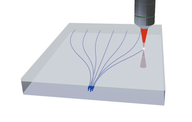
The TGV (Through Glass Via) glass substrate packaging technology is an innovative vertical electrical interconnection technology. By forming vertical micro vias on the glass substrate, it enables high-density interconnection between chips, and between chips and substrates. This technology originates from the TSV (Through Silicon Via) technology, but it uses glass as the substrate material, addressing issues such as high loss, high cost, and complex processes of traditional silicon-based interposers. The TGV technology has advantages such as excellent high-frequency electrical characteristics, large-sized ultra-thin glass substrates, superior mechanical stability, and good thermal conductivity. It is widely applied in fields such as sensors, CPUs, GPUs, AI chips, display panels, and advanced semiconductor packaging, driving the innovation of high-performance computing and chip packaging technologies.

More
3D Optical Waveguide

The laser direct writing 3D waveguide technology utilizes self-developed femtosecond laser direct writing equipment. By precisely controlling the laser writing on the glass substrate, it can achieve high-precision three-dimensional waveguide structures. This technology has the advantages of low loss, high density, and fine processing. It is capable of accurately controlling the propagation path of light at the micrometer level and is widely applied in fields such as optical communication, sensors, and optoelectronic integration. It promotes the innovation and development of optical communication devices and modules.

More

Events