Home>
Products & Solutions>
TGV Interposer tape-out OME Service>
TGV Optoelectronic Interposer Wafer(OEM Service)
TGV Optoelectronic Interposer Wafer(OEM Service)

Product Description
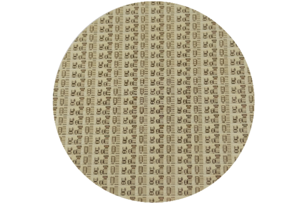
The TGV optoelectronic interposer wafer adopts an 8-inch wafer-level manufacturing process. Through laser-induced and deep silicon etching technologies, as well as the redistribution layer (RDL) and micro-bumping processes, it can support a maximum of 3+2 layers of RDL, achieving a wiring bandwidth of over 110GHz. It supports diverse application scenarios such as LPO, oDSP, and coherent optical communication, covering the needs from short-distance interconnection to long-distance transmission. It provides standardized solutions with 4/8/12/16 channels, is compatible with the pin definitions of mainstream optical chips (such as EML, VCSEL, silicon photonics, lithium niobate) and electrical chips (such as DML, DRV, TIA, DSP), and supports 2.5D/3D stacking and packaging technologies to achieve a high degree of integration in optoelectronic hybrid packaging. It can integrate the laser direct writing waveguide and the internal slotting structure of the interposer, and can support low-loss coupling with FAU, MT ferrules, MCF, etc., realizing high-density optical path fan-in and fan-out. It has the advantages of low crosstalk, high-speed signal integrity, and ultra-high integration, and can effectively solve the bottleneck problems of ultra-high-speed optical engine packaging, becoming a key technology for high-speed optical interconnection in the next-generation data center.
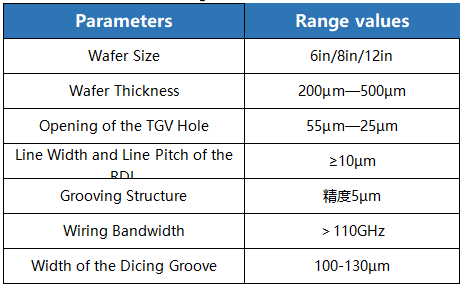
- Specification


