Exhibition time: March 17-19,2026
Venue: Los Angeles Convention Center
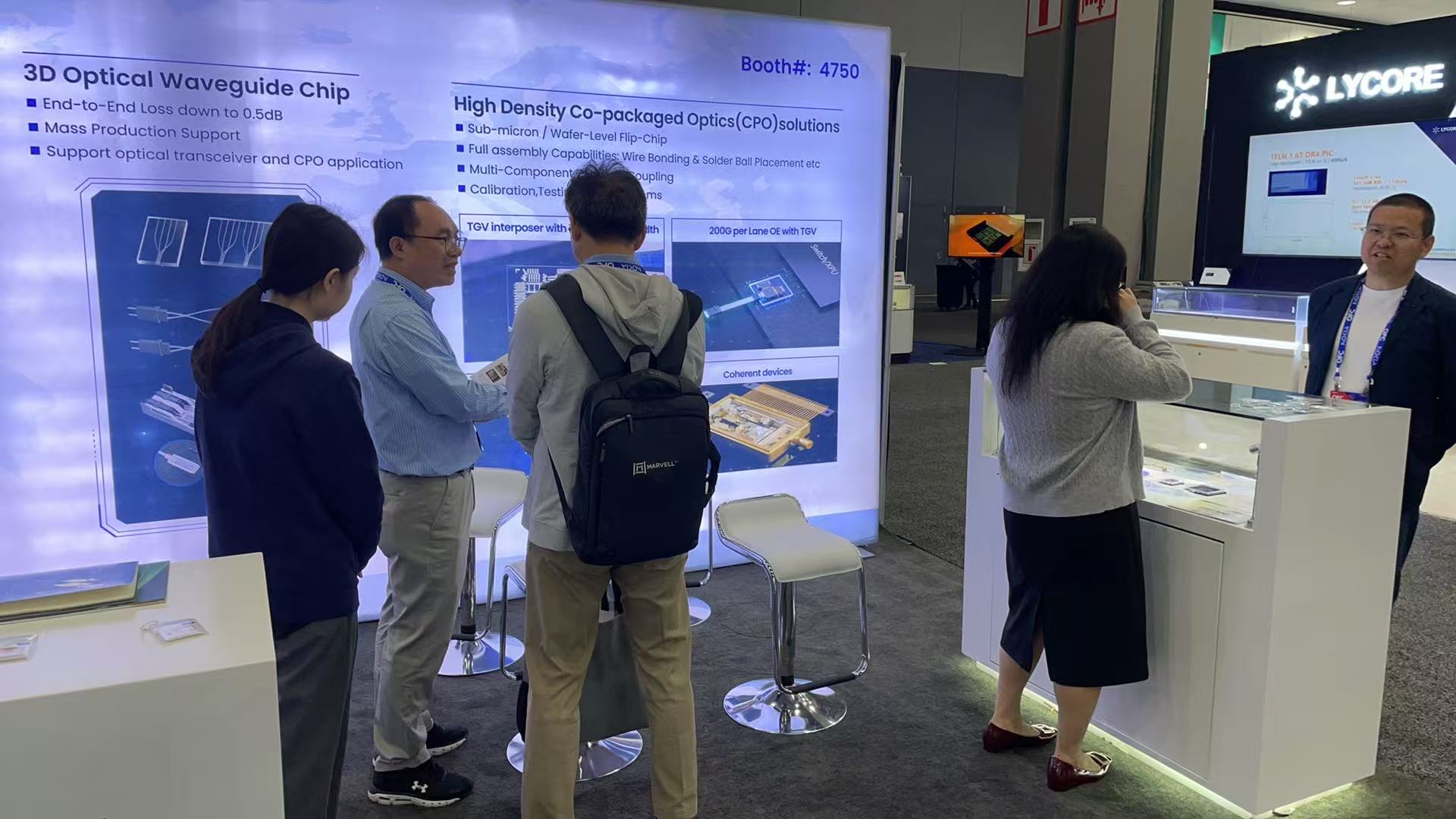
Booth number: WEST HALL, #4750
Part 1: 3D Optical Waveguide Chip
3D Optical Waveguide Chip Breakthrough for Data Center Interconnects
Driven by AI, large models, and HPC, data centers demand greater bandwidth density and interconnect efficiency. Optical interconnects are shifting toward higher speeds and integration—with modules advancing to 800G/1.6T and CPO architectures raising the bar for chip-level density. Traditional 2D planar waveguides face limits in channel density, space use, and routing flexibility.
In multi-core fiber (MCF) and CPO scenarios, high-density coupling and flexible optical routing in compact spaces are essential. 3D optical waveguide technology enables multi-layer optical paths in three dimensions, allowing signal transmission and crossover at varied heights and orientations. This boosts integration density and design flexibility, supporting MCF coupling and CPO interconnects—positioning it as a key enabler for next-gen data center optical solutions.
3D Optical Waveguide Chip Empowers Multi-core Fiber and CPO Applications
Shenzhen Photonics Valley (SPV) is set to showcase its latest innovation at OFC 2026: a series of glass-based 3D optical waveguide chips targeting next-gen high-density interconnects.
Designed to overcome the challenges of Multi-Core Fiber (MCF) and Co-Packaged Optics (CPO), the new chips deliver:
l For MCF: High-efficiency, low-loss optical coupling compatible with 4, 8, and 7-core fibers.
l For CPO: Advanced fan-in/fan-out solutions that enable precise 3D routing for high-density photonic integrated circuits.

3D Optical Waveguide Chip Series
Product Highlights: Superior Performance Indicators and Mass Production Capability
SPV will unveil its glass-based 3D optical waveguide chips at OFC 2026, leveraging proprietary femtosecond laser direct writing technology to fabricate high-precision 3D optical paths within glass substrates—ideal for multi-core fiber (MCF) and CPO applications requiring ultra-high interconnect density.
The chips deliver exceptional optical performance, with waveguide transmission loss below 0.1 dB/cm and end-face coupling loss under 0.25 dB/face. For a standard 4-core waveguide chip converting pitch from 127 μm to 40 μm, fiber-to-fiber insertion loss is controlled within 0.5 dB, ensuring excellent channel uniformity and stable coupling. These metrics meet the stringent low-loss requirements of next-gen 800G and 1.6T optical interconnect systems.

Key Performance Indicators of 3D Optical Waveguide
SPV has completed its glass-based 3D optical waveguide chip production line as of August 2025. Equipped with in-house developed femtosecond laser direct writing systems and high-precision automated coupling test platforms, the line enables second-level waveguide processing with exceptional efficiency and consistent quality, ensuring reliable volume production for large-scale deployment in data centers and CPO systems.

3D Optical Waveguide Chip Production Line
Event Highlight: Industry Synergy in Action: First-Ever Joint Demo of 3D Waveguide Samples.
SPV is driving industrial chain synergy through deep collaboration with downstream passive component manufacturers, yielding strong early results. At OFC 2026, the company will team up with industry partners to jointly unveil the latest prototype built on 3D optical waveguide technology.

✨ MT+MCF FIFO based on 3D Waveguide ✨
This integrated sample set brings together expertise across chip design, 3D waveguide fabrication, and passive packaging, demonstrating end-to-end industrial chain collaboration. Built on SPV's 3D optical waveguide chips, the solution achieves efficient fan-in/fan-out (FIFO) optical connections between silicon photonic chips and multi-core fiber MT ferrules—meeting the demands of 800G/1.6T/3.2T multi-core optical modules and providing a comprehensive chip-to-device solution for next-gen high-density interconnects.
During OFC 2026, SPV's technical team will showcase this joint prototype alongside its full 3D waveguide product lineup. We warmly welcome optical module and fiber manufacturers, passive device suppliers, data center operators, and industry partners to visit our booth for discussion and collaboration on the future of high-speed optical interconnect technology.
Part 2: Advanced Packaging Services
Zhejiang LayChip Optoelectronics, a wholly-owned subsidiary of Shenzhen Photonics Valley (SPV), specializes in advanced glass-based TGV and CPO technologies. Headquartered in Wenling with a 5,000㎡ modern facility including 2,000㎡ of high-standard cleanroom, the company delivers precision manufacturing capabilities across wafer-level packaging to module assembly.
Core Packaging Capabilities
Leveraging advanced glass-based TGV technology, LayChip Optoelectronics overcomes the bandwidth and power constraints of traditional packaging:
l High-Density Interconnect: Glass substrates enable micron-scale via interconnects, supporting 2.5D/3D stacked packaging with superior high-frequency performance.
l Ultra-Low-Loss Transmission: Optimized for AI computing and supercomputing centers, the solution supports high-speed optical interconnects from 800G to 3.2T while significantly reducing signal latency and power consumption.
l Co-Packaged Optics (CPO): Delivers high-precision co-packaging of silicon photonic (PIC) and electronic chips (EIC), providing high-integration, high-reliability optical engine solutions.
Product Showcase at OFC 2026 – Advanced Packaging
At OFC 2026, LayChip Optoelectronics will unveil its ELSFP (External Laser Source Fitting Package), demonstrating high-efficiency light source coupling enabled by advanced packaging technology.
Designed as a "plug-and-play" standalone light source, the ELSFP delivers high-power, high-stability optical solutions for next-gen data center interconnects. It effectively addresses thermal management and maintenance challenges inherent in CPO architectures, providing a reliable and easily integrated light source for co-packaged optical engines.

ELS modular product image
March 17-19 at Los Angeles Convention Center. We look forward to seeing you!