


Home>
Products & Solutions>
TGV Interposer Chip>
TGV Optoelectronic Interposer Solution OEM Tape-out Service
TGV Optoelectronic Interposer Solution OEM Tape-out Service

Product Description
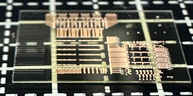
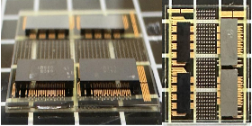
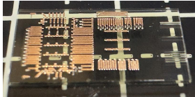
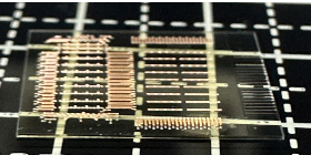
Based on the mature and reliable 8-inch wafer-level manufacturing process, Shenzhen Optical Valley Technology can realize TGV interposer wafers that support wiring bandwidths above 110GHz through laser induction, deep silicon etching and rewiring (RDL), and micro-bump processes; it provides 4/8/16-channel standardized solutions, compatible with the pin definitions of mainstream optical chips (such as EML, VCSEL, silicon photonics, lithium niobate) and electrical chips (such as DML, DRV, TIA, DSP), and uses laser direct writing optical waveguide technology and 2.5D/3D stacking packaging technology to achieve high integration of optoelectronic hybrid packaging; while supporting wafer-level TGV interposer customization, it can MPW customize multi-solution wafers, significantly reducing the cost of large-scale production. With the advantages of low crosstalk, high-speed signal integrity and ultra-high integration, it can effectively solve the bottleneck problem of ultra-high-speed optical engine packaging and become a key technology for high-speed optical interconnection in the next generation of data centers.
- Specification
Related Products